A TDS sensor (Total Dissolved Solids) is used to measure how many dissolved solids are in water, helping us understand its quality. TDS refers to the total amount of substances like salts, minerals, and metals that are dissolved in the water. The sensor works by checking how well the water conducts electricity. Since dissolved solids, such as ions, make water conduct electricity better, the TDS level can be determined by measuring this conductivity.
TDS Sensor Modules
Gravity Analog TDS Meter
When using an Arduino to measure Total Dissolved Solids (TDS), the most commonly used sensor is the Gravity Analog TDS Sensor Kit developed by DFRobot. This sensor is popular due to its simplicity, accuracy, and compatibility with Arduino. For comprehensive information about the Gravity Analog TDS Sensor by DFRobot, you can refer to the official DFRobot Wiki page: DFRobot Wiki
Grove - TDS Sensor
The Grove – TDS Sensor by Seeed Studio is another popular choice for measuring Total Dissolved Solids (TDS) with an Arduino or other microcontrollers. It is part of the Grove ecosystem, known for its modular, plug-and-play design, making it ideal for beginners and professionals alike.
For comprehensive information about the Grove – TDS Sensor, including its specifications, setup instructions, and example code, you can refer to the official Seeed Studio Wiki page: Seeed Studio Wiki
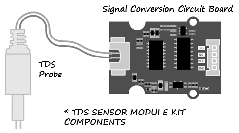
TDS Sensor Kit Components
Both sensor kits contain the following key components:

TDS Probe:
- A waterproof electrode that measures the conductivity of water.
- Two metal electrodes are used to create an AC signal for testing the water’s conductivity.
Signal Conversion Circuit Board:
- Converts the water conductivity into an analog voltage.
- Outputs a signal that can be read by the Arduino’s analog input pins
TDS Sensor Module Schematic | 5-Step Guide
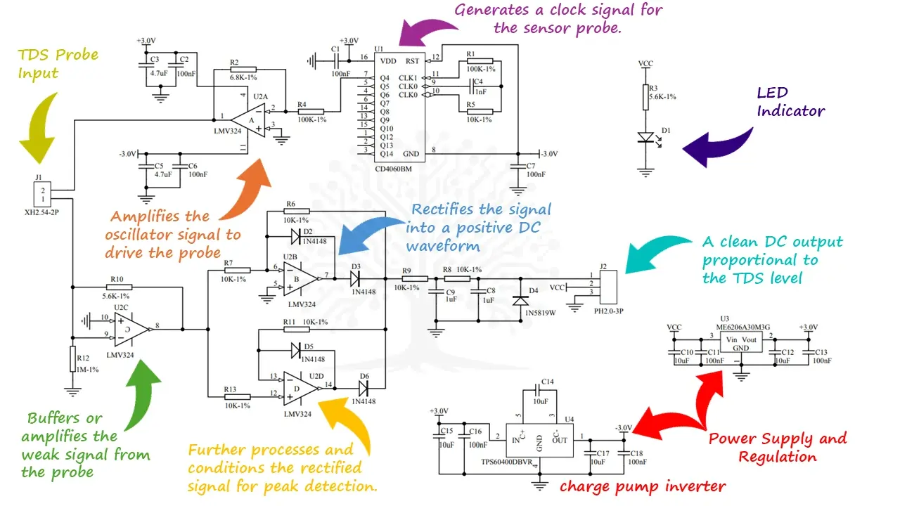
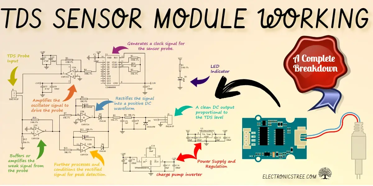
Based on the schematics provided by both product manufacturers, the Grove TDS Sensor and Gravity TDS Sensor appear to share the same core circuit design. This is likely because both implement the same principles of AC signal generation, amplification, and rectification for TDS measurement. Therefore, we will focus on the Gravity sensor schematic and explain how it works.

Power Supply Section
The circuit requires both +3.0V and -3.0V to power the operational amplifiers and ensure bipolar operation for signal conditioning. To achieve this, U3 (ME6206A30M3G), a 3.0V linear voltage regulator, converts the input VCC to a stable 3.0V supply. Capacitors C10, C11, C12, and C13 provide input and output filtering to stabilize the voltage supply. Additionally, U4 (TPS60400DBVR) is a charge pump inverter that generates a negative voltage (-3.0V) from the +3.0V input. Filtering capacitors C14, C15, C16, C17, and C18 help maintain stable input and output voltages.
Oscillator and Probe Signal Generation
U1 (CD4060) generates an alternating current (AC) signal that drives the two electrodes of the TDS probe. Why AC? Using AC instead of DC prevents electrode polarization, which occurs when ions accumulate on the surface of the electrodes under DC. Polarization can degrade the accuracy of the measurement.
f = 1 / (2.3 × R_total × C)
Where:
- R_total = R1 + R5 (resistors in the timing network, values given in the schematic).
- C = C4 (timing capacitor, value given in the schematic).
Values from the schematic:
- R1 = 100kΩ
- R5 = 10kΩ
- C4 = 1nF (1000pF)
The resistors R1 and R5 are in series for the timing network:
R_total = R1 + R5 = 100kΩ + 10kΩ = 110kΩ
Substitute the values into the formula:
f = 1 / (2.3 × 110,000 Ω × 1 × 10^(-9) F)
f = 1 / (2.53 × 10^(-4))
f ≈ 3.95 kHz
The AC signal frequency generated by the CD4060BM is approximately 3.95 kHz.
TDS Sensor Interface
J1 is the connection point for the TDS sensor. The sensor measures the conductivity in water, which is proportional to the total dissolved solids. The AC voltage generated by the CD4060BM drives the TDS sensor, and the resulting signal is then conditioned by the op-amp stages for further processing.
Operational Amplifier Stages
U2A – Signal Amplification (Excitation Signal for the Probe)
- U2A amplifies the square wave signal from the oscillator (CD4060BM) and ensures the TDS probe receives a high enough signal amplitude to function properly. The gain of the amplifier is set by R2 (6.8kΩ) and R4 (100kΩ).
The gain is calculated using the formula Gain = − (R4 / R2), which gives a value of approximately -14.7.The gain is R2/R4 (not R4/R2) that gives a gain lesser than 1. ( Corrected By: Gianni )
The amplified signal is then sent to the TDS probe through the output of U2A.
U2C – Differential Signal Amplifier (Probe Signal Input)
- U2C processes the signal coming back from the TDS probe. It’s most likely configured as a buffer or differential amplifier to handle the raw signal, which contains the conductivity data. The resistors R10 (5.6kΩ) and R12 (1MΩ) likely set the input impedance and bias point for the op-amp. R10 is also part of the feedback loop, allowing for proper buffering or gain adjustment of the signal.
U2B – Signal Rectification (Half-Wave Rectifier)
- U2B works alongside diode D2 (1N4148) as a half-wave rectifier to convert the AC signal from the TDS probe into a positive DC signal. The resistors R6 and R7 (both 10kΩ) help control the current and provide feedback to ensure the circuit functions correctly. Diode D2 (1N4148) only lets the positive half of the signal pass through, effectively rectifying the AC signal.
U2D – Signal Conditioning and Peak Detection
U2D converts the fluctuating rectified signal into a steady DC signal that is proportional to the TDS level. It further processes the probe signal to ensure accurate peak detection and proper DC level extraction. R11 and R13 (10kΩ each) configure the feedback loop and set the input impedance. D5 and D6 (1N4148) form a diode-based rectification circuit that handles the signal peaks, ensuring the signal is properly rectified for reliable DC output.
Diode Protection and Output
D4 (1N5819W) is a Schottky diode used for protection, ensuring voltage stability and preventing damage to the circuit. The final signal, which is a DC voltage proportional to the conductivity, is available at J2. This signal can then be fed into an ADC (Analog-to-Digital Converter) of a microcontroller for further processing. The microcontroller can apply the TDS conversion factor to calculate the TDS value in ppm.
TDS Sensor Module Circuit Functionality Overview
The TDS sensor module operates by using an AC signal generated by the CD4060, which drives the TDS probe. The current that flows through the water, as measured by the TDS probe, is directly proportional to the concentration of total dissolved solids (TDS). The op-amp circuits then amplify, rectify, and filter this signal, converting it into a clean DC voltage. This resulting voltage is proportional to the TDS level in the water and is sent to the output for further processing, such as being fed into an ADC for digital conversion and TDS calculation in ppm.


Pingback: New TDS Sensor Module Library Proteus 8 | Free Download - ELECTRONICS TREE
I question the gain calculation of U2A. It appears to be the inverse of the stated gain. Comments?
You’re right, the gain is R2/R4 (not R4/R2 as stated in the article) that gives a gain lesser than 1: in fact gain is 0.068. I’ve the sensor and I measured input an output values with an oscilloscope and I have a voltage output of about -0.2V when input is 3V: just like (right) calculations suggests
And…anyway an amplifier cannot produce a voltage output greater than the power supply value: the input voltage is 3 or -3V (due output of CD4060 that is a pure square wave) so a gain of 14 means a voltage output of from -42 to 42V that is impossible since amplifier is powered at 6Vpp
Gianni, thank you for the correction. I didn’t notice that I swapped the resistor values. If the feedback resistor (R2) is less than the input resistor (Rin), the amplifier will attenuate the signal. I’ve corrected this in the article with your reference and also removed my previous statement.
I also measured frequency output from the CD4060B and I have about 2.4Hz. Following the Texas Instruments CD4060B datasheet, Period from the RC is calculated as 2.2 * Rx * Cx, where Rx is the resistor connected on pin 10, the resistor connected on pin 11 must not be used for calculations and it’s only needed to be from 2 to ten times greater than Rx, so Period is 0,000022 seconds, corresponding to 45,4kHz, circuit takes output from Q4 pin so frequency must be divided by 16, so final frequency must be around 2,8kHz that is nearest to the value I find experimentally. Using a value of 2.5 instead of 2.2, as other datasheets reports, lead to a frequency value from Q4 of 2,5kHz that is even near to what I find
but why we use attenuated gain from U2A I did not understand this point and in that way we are getting attenuated value around 240mv and -240mv